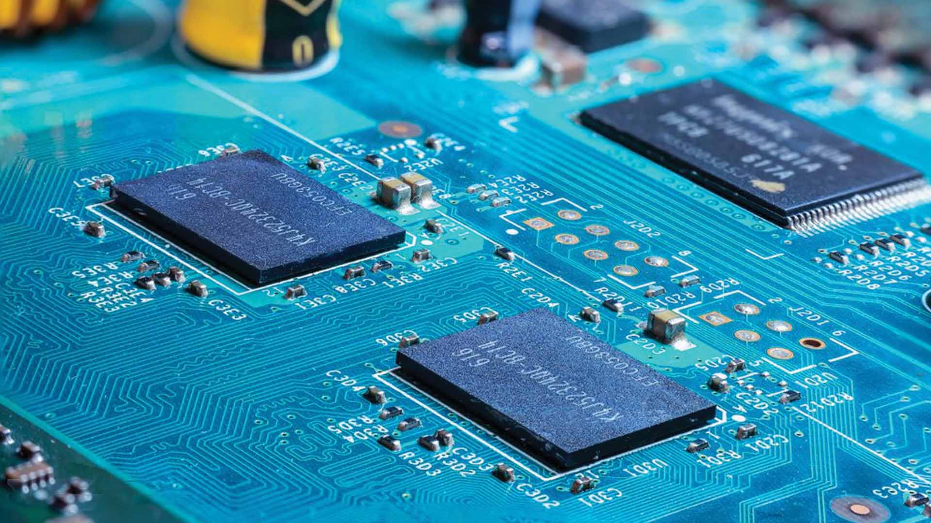
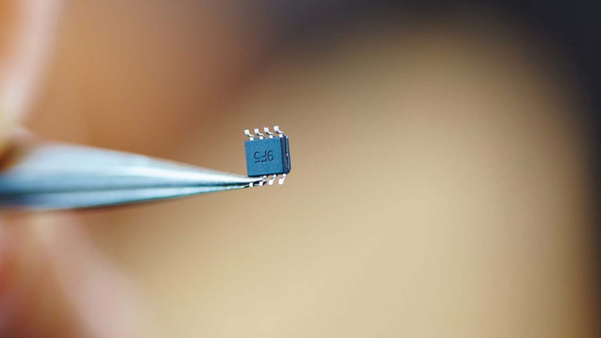
In 2018, Apple began production on a new generation of microchips for iPhones. The computer company and Taiwan Semiconductor Manufacturing Co. went to work on the A12, a 7-nanometer design that’s smaller and more efficient than the current 10-nanometer chip. This is all well and good, except one tiny thing: how are microchips manufactured?

It starts with, of all things, sand. Normally, you’d want to keep sand far away from your electronics, particularly your phone. However, sand is one of the main components of silicon. Silicon is one of the most common elements on Earth, with about 28% (by mass) of the crust being composed of it. It’s also a semiconductor, meaning it conducts electricity under certain conditions. This makes it vital for integrated circuits, especially microchips.
The silicon must be processed before it can be used, however. It reaches 99.999% purity (also called “five 9s”) through chemical processes. Heat is used to create a purified silicon melt before it’s grown into a monocrystalline ingot. These ingots are massive, measuring up to seven feet in length and weighing 1,000 pounds. The ingots are sliced into super-thin wafers, less than 10 human hairs thick. However, the diameter of the wafers can range anywhere from four to eighteen inches. The wafers are then polished until they’re smooth and mirrored.
The wafer then undergoes a complex process, so the chip design can be transferred onto the wafer. Photolithography is used to project each of the thousands of layers onto the wafer. Each layer of the chip is electrically connected to the next with billions of transistors, and each circuit pattern is unique. A DUV (deep ultraviolet) light source is used to make the etching, much like the exposure step in photography (hence the name).

Each layer of the microchip is etched, polished, and integrated. Non-silicon elements, known as dopants, can be used to further modulate the electrical properties of each layer. When exposed to the proper amounts of other elements and heat and pressure, the silicon reacts by adjusting its conductivity. This step is essential for ensuring the chip works as intended and isn’t in danger of using too much/too little charge.
The conductive paths between layers are achieved by having the whole microchip be coated in metal, usually aluminum. The photolithography process is used again to remove all but the conductive pathways. For larger microchips, this may also involve multiple layers of conductors separated by glass.
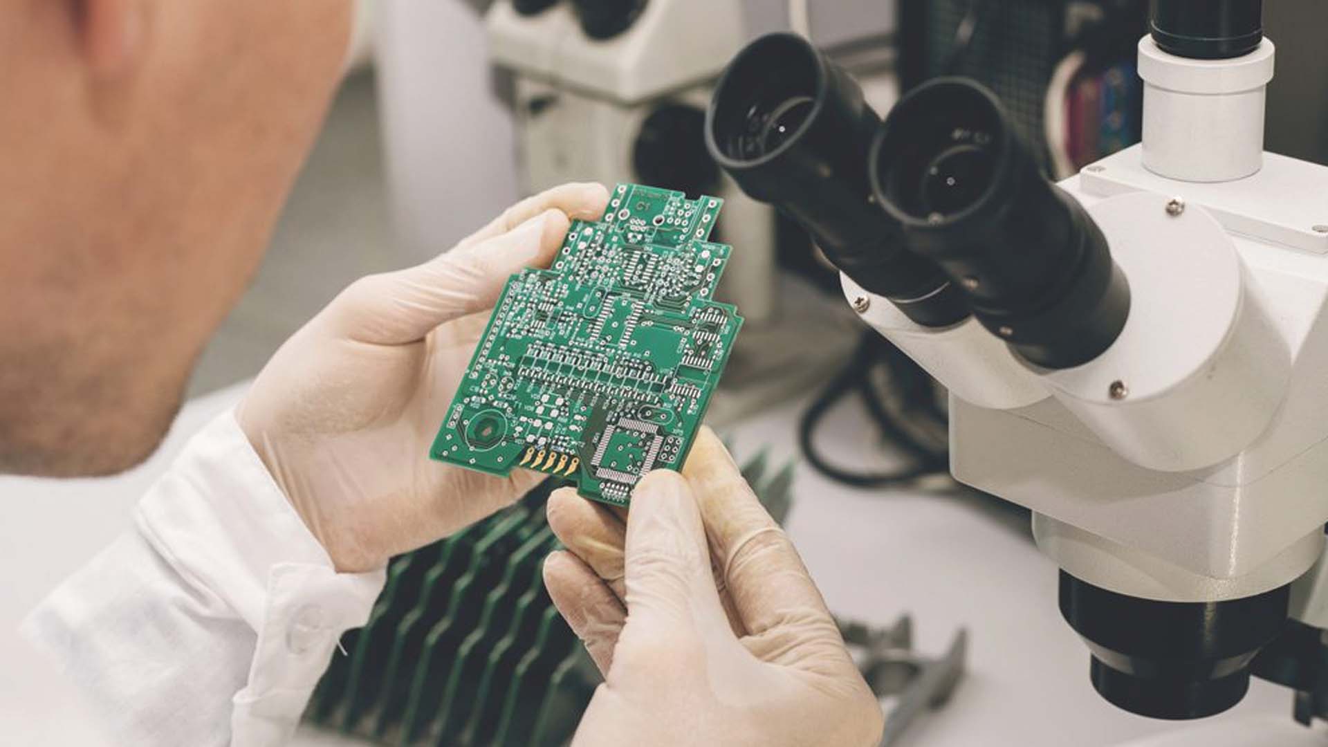
Each individual spot on the is tested for functionality. If even one die isn’t working properly, the entire microchip must be discarded. But if all parts are functional, it’s noted and marked and moved onto the final step: packaging. The wafers are cut ultra-thinly and wires are attached. It’s further encased to protect from damage. The final product is the integrated chip found in all electronic devices.
In the case of cell phones, the process is virtually identical to that of creating microchips for laptops or game consoles. The only real difference is the overall size of the chip. Given that smartphones are much smaller than your average PC or tablet, the chip needs to be even smaller. This does mean sacrificing some of the processing power, but they’re still plenty dedicated enough to keep up with all we demand of our phones.

Making a microchip is expensive, difficult, and the driving force of electronics and the economy. Only four companies produce chips for all the devices that power our lives, including the aforementioned TSMC. They look deceivingly trivial and come from simple sources, but don’t be fooled. Microchips are a very, very big deal in a very, very tiny package.
Learn more about the World of Production, and discover how artificial trees, life jackets, and the Nintendo Switch are made.


